Building an SMPS from scratch
Designing and building an SMPS (Switch-Mode Power Supply) from scratch is no small feat. Our goal: Create an SMPS with completely isolated outputs at standard voltages (+12V, -12V, +5V, -5V, and +3.3V), each capable of delivering up to 1A. The input would be standard AC mains voltage. Here’s an account of how we achieve this—complete with calculations, rewinds, and a few twists.
We tried multiple different design documents, and referred to multiple YouTube videos, but nothing worked, until Raghumanth A suggested and handed us a design document.
Calculation Workbook & Reference documentation can be found below
The Design
Our first step was designing the flyback transformer, the heart of the SMPS. This began with calculating the load occupancy factor for each output.
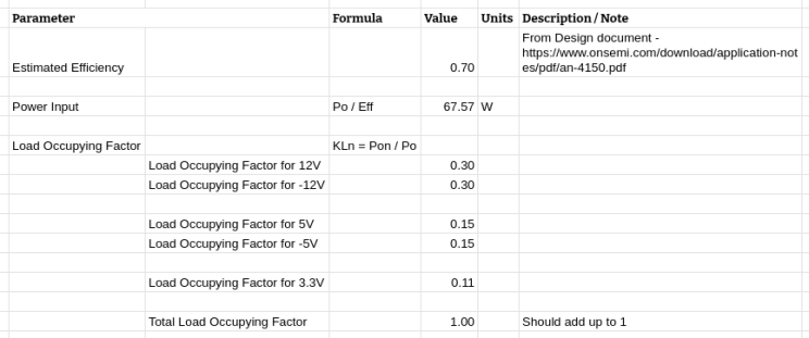 Calculating the Load Occupying factor
With these factors in hand, we estimated the reflected output voltage on the MOSFET and included a safety margin.
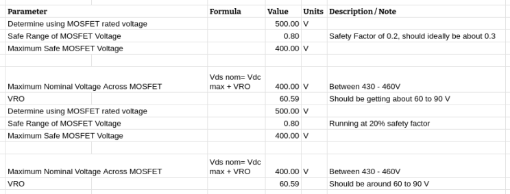
We then went ahead trying to get the required components, and found a couple of different MOSFETs.
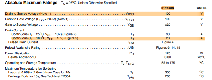 IRF540N - Maximum drain to source voltage of \(100V\) & Peak continuous current of \(23 A\)
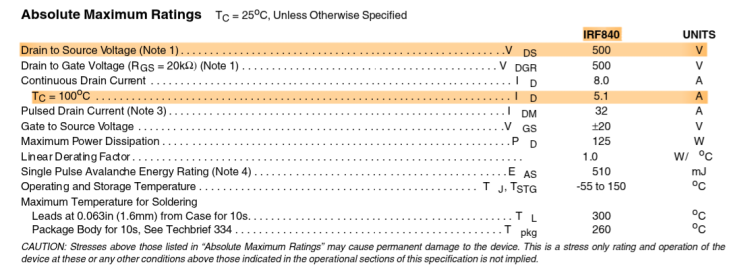 IRF840N - Maximum drain to source voltage of \(500V\) & Peak continuous current of \(5.1A\)
The choice was clear—we needed the IRF840N to handle the reflected voltage safely. The choice was clear—we needed the IRF840N to handle the reflected voltage safely.
Transformer Design
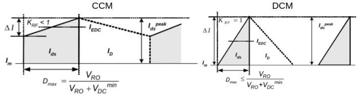 Difference in the currents of CCM vs DCM
Out of the two modes of operation, we opted for the CCM (Continuous Conduction Mode) and calculated the inductance required on the primary winding.
 Primary inductance of \(614 \mu H\)
We then took an additional step to verify that our MOSFETs current ratings were well above the the currents that we would be driving through it.
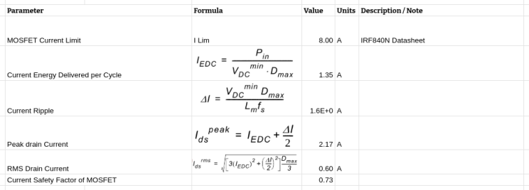
Ensuring an adequate safety factor for current ratings, we finalised the EE42/15 core, which provided the necessary balance between size and performance, out of the cores we had available. We then calculated the minimum number of primary turns required on the primary side.
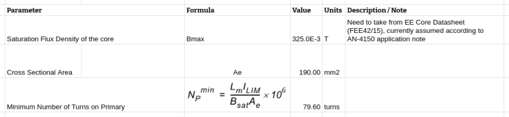 Calculated the minimum number of turns
Then calculated the number of turns of the reference on the secondarys, and based on that calculated the turns ratio for the other voltage windings. Keeping the ratio constant we ensured the get the turns to an integral number.
For the reference voltage, we chose \(2.5V\), aligning it with the Arduino ADC midpoint. This allowed sufficient flexibility in duty cycle adjustment while protecting the microcontroller.

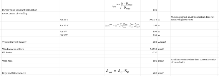
With the reference set & the turns calculated, we determined the wire gauge. Although we needed \(1.00mm^2\) copper wire, we used a \(1.5mm^2\) wire available in our lab, and verified that the bobbin fit through careful planning.
Winding the Transformer
We realised that winding the transformer was both art and science. While meticulously counting the number of turns, I lost track of the dot convention (indicating winding start and end), and the coils weren’t wound neatly, which meant the bobbin didn’t initially fit into the core, and had to be rewound several times to ensure a proper fit.
Post winding, was when the realisation hit, that the dots (from the dot convention was lost), so we checked the output on the secondary windings while applying a \(2 VAC\) to the primary.
Finally, we measured the inductance on the primary, and found it to approximately match, with an error of about \(30\mu H\)
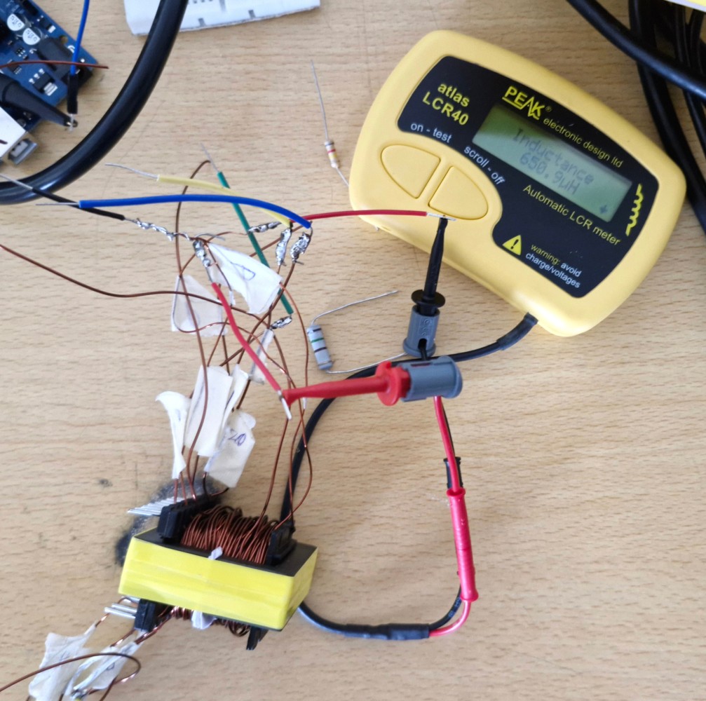 Primary inductance of \(650\mu H\)
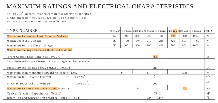
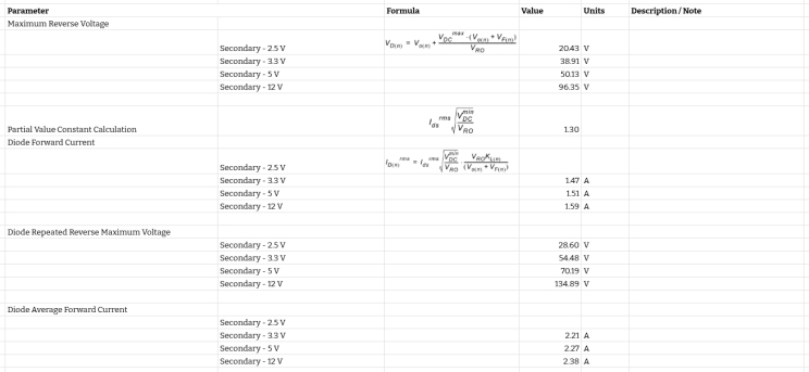
With the transformer ready, we selected suitable diodes & capacitors on the secondary side for smoothening out the secondary voltages. From the available selection of diodes, we picked the MUR460, as the maximum repeated reverse voltage was well above threshold, but more importantly, the reverse recovery time was short.
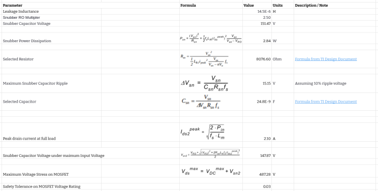
Initially, we tried the snubber circuit that was suggested by the design document, but it didn’t work as expected, casing excessive ripples in the voltage across the MOSFET. After consulting our professor Rex, we implemented the snubber circuit he suggested, which worked perfectly. Thanks to the TI Application note, the calculations went smoother.
Assembling and Testing
Bringing everything onto a perfboard, we faced another hiccup: The next challenge arose with the gating circuit, where grounding issues caused improper operation.
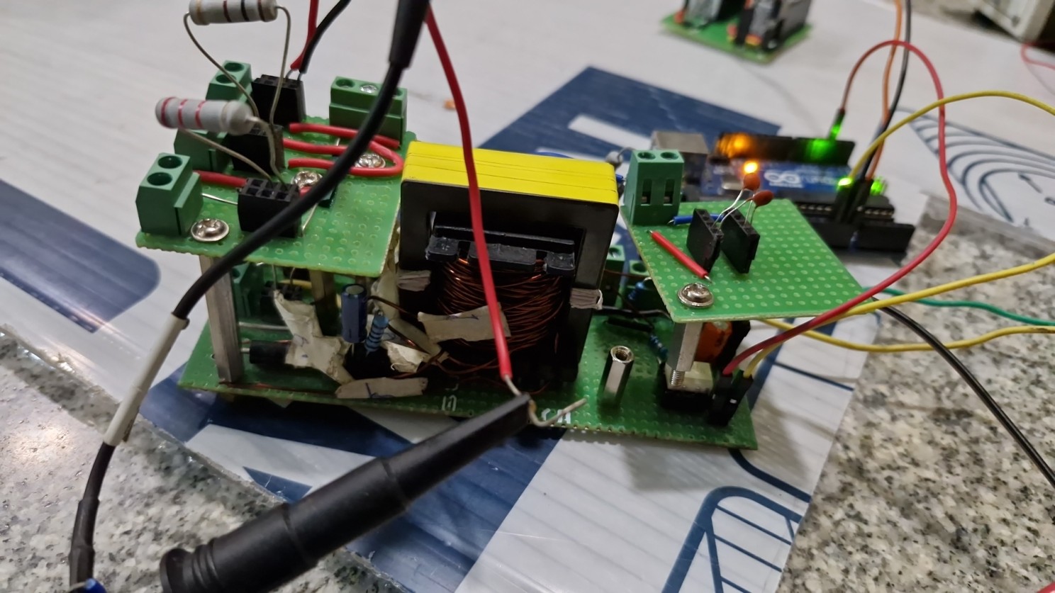 Final perfboard setup
Resolving this brought the circuit to life. Testing various loads confirmed the outputs aligned with our design goals.
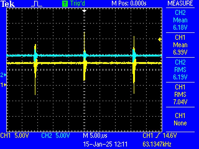 ~7V outputs on 5V channel
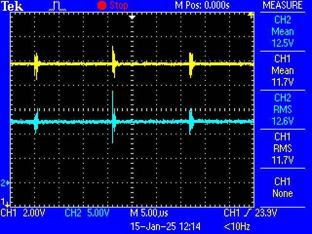 12V output on 12V channel
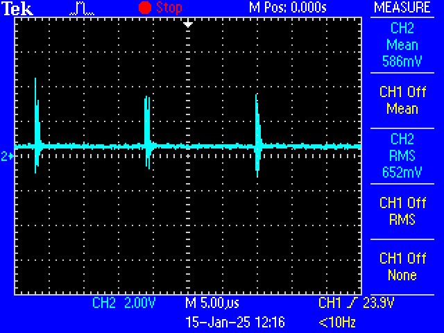 Reference channel, 2.93V on 3.3V channel (Voltage divider of 5:1)
We faced yet another hiccup: The Arduino’s 8-bit timer lacked the resolution for precise control, leading to slow response times and difficulty in achieving stable regulation. Thus, the need to pick a different development board arose. With its higher-resolution timer, the Raspberry Pi Pico allowed for finer adjustments in duty cycle modulation, resulting in a more responsive and stable output voltage. This improvement was crucial in maintaining precise voltage levels across varying loads, ensuring optimal performance of the SMPS.
To safeguard the Pico’s ADC, a simple 3V OpAmp clipper circuit was implemented and placed between the reference winding and the ADC.
With the limited time, we partially tuned the PID Controller. Though it took a while to stabilize, it consistently reached the desired output voltages, somewhat.
| Expected Output | Output | Error |
|---|---|---|
| 12V | 12.5V | +0.5V |
| -12V | -11.7V | -0.3V |
| 5V | 6.18V | -1.18V |
| -5V | -6.99V | -1.99V |
| 3.3V | 2.93V | 0.37V |